
Low-Energy Electron MicroscopyIn low-energy electron microscopy (LEEM), the electrons elastically scattered from a surface are imaged -using electron optics- onto an area detector [1]. This scattering is the very same process that gives rise to low-energy electron diffraction (LEED). As such, LEEM was invented by Ernst Bauer as a natural extension of LEED. A direct advantage is that any LEEM instrument is capable of performing both microscopy and diffraction with equal ease.
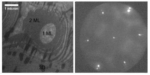 Figure 1: A nice example of mesoscopic texture probed by low-energy electron microscopy: Fe film grown on the W(110) surface. As seen in the LEEM image on the left, the initial layer-by-layer growth is followed by the formation of 3-dimensional islands (Stranski-Krastanov type growth). Its low-energy electron diffraction pattern is displayed on the right. The single layer is pseudomorphic to tungsten, whereas the 3D islands can be identified with the LEED spots corresponding to a relaxed Fe(110) surface.
LEEM optics (which allow a spatial resolution of about 10 nm) can be used, without any additional modification, to image photoemitted electrons from a surface illuminated by a photon beam. With an energy filter built into the instrument, the result is photoemission microscopy (PEEM) [2,3]. In addition, imaging the diffraction pattern (just as in LEED) makes it possible to measure the photoelectron diffraction from a micron-sized region on the surface. No less important is absorption microscopy, which also can profit from the well-defined polarization of synchrotron light to allow magnetic microscopies (XMCD/XMLD). A combination of all these techniques make LEEM a powerful facility for surface science studies.
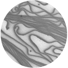 Figure 2: Another example of Fe growth on W(110). In this case, the W(110) surface is partially covered with oxygen. The tendency of Fe monolayer to grow from the atomic steps (step-flow) and to stay away from oxygen covered areas results in the beautiful pattern displayed. The size of the image is 5 microns.
[1] E. Bauer, "Low-Energy Electron Microscopy", Rep. Prog. Phys. 57, 895 (1994).
[2] A. Locatelli, L. Aballe, T. O. Menteş, M. Kiskinova, E. Bauer "Photoemission electron microscopy with chemical sensitivity: SPELEEM methods and applications", Surf. Interface Anal. 38, 1554 (2006).
[3] A. Locatelli and E. Bauer, "Recent advances in chemical and magnetic imaging of surfaces and interfaces by XPEEM", J. Phys.: Condens. Matter 20, 093002 (2008). |
